
Recently I started work on a new board. This one will be a front door entry system, so I decided to go with something that could read my NFC implant but also had a numeric keypad for the kids (and anyone else) to use. Not everyone wants to be chipped. Crazy, isn’t it? I’ll write more up on the board when it gets closer to completion, but for this post I’m going to concentrate on a small PCB antenna that’s intended for use with a tiny implanted tag. I’ve successfully used a wirewound inductor before, but I decided it was time to try a PCB trace antenna. This is the most common way to make an NFC reader, but nobody seems to have tried to tune one for an implant – probably because it means it will be worse at reading larger tags. Anyway, this is about creating a small PCB antenna and more importantly tuning it so that it read well.
 So, this is the PCB. It’s based around a MSP430FR2633 for it’s great capacitive sensing for the buttons. There is also a TRF7970A NFC transceiver as I’m familiar with this. You may also notice that I’ve gone for a reverse mount RGB LED that shines through that unmasked piece of the board. I’m really pleased with how that works. Check out this video of the buttons in action to see if you agree.
No VNA?
The NFC part also worked fine, but I must admit the range and sensitivity wasn’t great. I had calculated that the PCB antenna should have an inductance of about 1μH so I just used the same matching components that worked well previously. What I really needed to tune the matching circuit was a Vector Network Analyser (VNA). Unfortunately these are very expensive and I’d likely only ever use one for this. Is there another way? Well, luckily I came across an article entitled “Impedance matching for 13.56 MHz NFC antennas without VNA” which seemed to be just what I was after. Then only slight problem was that I needed an accurate measurement of the impedence of the PCB trace – by which I mean it’s inductance and resistance. I needed to buy a slightly less expensive piece of equipment – an LCR meter. I went for the DER DE-5000 which I must say I’m extremely happy with.
Measuring and calculating
So it turns out that the PCB trace I expected to be about 1μH turned out to be 0.627μH with a resistance of 0.867Ω – otherwise expressed as 0.867 + j53.42Ω. The article suggested a parallel resistor of 362Ω so i went with the closest I had of 470Ω. Calculating the parallel and series capacitances seemed trickier. I ended up using some Smith Chart software from Fritz Dellsperger. and to be honest I sort of went with trial, error and adjustment to try to get the final point as near to 50Ω as possible. I managed a theoretical 54.973 – j1.455Ω
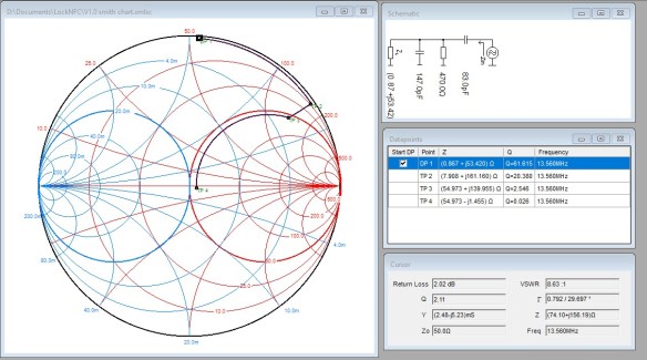
I approximated the parallel capacitance to 100μF + 47μF = 147μF and the serial to 68μF + 15μF = 83μF. With the measured value of my PCB trace and the matching components I had it had been 8.847-j135Ω. No wonder it wasn’t great!
The end result
Whilst reworking the board I measured the lowish tolerance capacitors I was using and by selecting the most appropriate ones I ended up a little bit closer to my goal. Did it work? You bet it did. I must admit I was surprised how well. Just as I was surprised when the reader and keypad worked too. Maybe I should have a bit more confidence in these things (and myself).

Pingback: Near field antenna tuning without a Vector Network Analyser (VNA) « Adafruit Industries – Makers, hackers, artists, designers and engineers!
That is amazing! really REALLY cool to see it all integrated into one PCB!
You stated that the reader should be worse at reading the larger tags for the non-cyborg units out there. would they still work? and what about keyfobs?
I just tried it. It’s much as I expected.
Coupling with smaller tags like keyfobs, etc. works just fine as they’re fairly similar in size to my reader’s antenna. For larger credit-card sized tags it seems that you have to get the edge of the card (where the coil is) right over the PCB antenna. It’s just like the way you have to get an implanted tag right onto the large PCB trace of most readers.
Very nice. For better matching you should measure the resistance at 13.56Mhz to get the Skin effect of your pcb antenna into the equations. They do add a significant amount that can throw up your matching unless you go big PCB traces (which I suggest you should do).
Pingback: NFC antenna tuning without a VNA – gStore
Pingback: A Journey Through NFC Antenna Tuning Without a VNA | iotosphere - Internet of Things
Big like!
Always wanted to do something like that for my implant, but lack of VNA held me back..
Hello,
Great work!
The max. frequency available for DER DE-5000 is 100kHz. Were you using this frequency to measure your inductance of the NFC antenna?
Would it be alright to describe briefly how you do the measurement for inductance and resistance?
Thank you.
The measurement at 100kHz didn’t seem to be a problem. It was fine by using the DE-5000 and a good multimeter as normal.
To be honest, the NanoVNA has appeared since I wrote this. It works very well at 13.56MHz. I’d really recommend it. I’ll have to write that up when I get a chance.